Stop Prototyping Forever: How to Graduate From Breadboards to Your Own Custom PCB
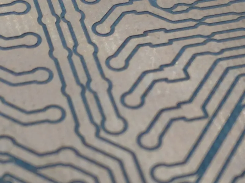
Photo: Nicola Corna, CC BY-SA 4.0, via Wikimedia Commons
There's a rite of passage in the maker world that nobody really warns you about. You've built something cool on a breadboard — maybe a custom sensor array, a motor controller, or a little weather station — and it actually works. Then you pick it up to move it, a wire pops loose, and suddenly your masterpiece is a pile of jumper spaghetti again.
That's usually the moment people start Googling "how to design a PCB."
Custom circuit boards used to be strictly the domain of electrical engineers with expensive software licenses and corporate fab accounts. That's not the world we live in anymore. Between free EDA tools, dirt-cheap overseas fabrication, and a huge online community of makers who've already figured out the hard parts, your first custom board is way more within reach than you might expect. Let's walk through exactly how to get there.
Why Bother? The Real Case for Going Custom
Before we talk tools and technique, it's worth being honest about when a custom PCB actually makes sense. If you're building a one-off project that you'll never replicate, a well-organized breadboard or even some perfboard with soldered connections might genuinely be the better call. Custom boards cost money and time upfront.
But if you're building something you want to be reliable, portable, or reproducible — a PCB pays for itself fast. Connections are permanent. The form factor is exactly what you need. You can share your design files with the community or even sell kits. And honestly? There's a satisfaction to holding a board with your own name silkscreened on it that's hard to put into words.
For projects like wearables, robotics, custom keyboards, or any embedded system that lives in an enclosure, a custom board isn't a luxury. It's the logical next step.
Picking Your EDA Tool
EDA stands for Electronic Design Automation — basically, the software you use to design your schematic and lay out your board. There are three names you'll hear constantly:
KiCad is the go-to for most hobbyists and independent makers. It's completely free and open-source, runs on Windows, Mac, and Linux, and has a massive library of components. The learning curve is real, but the community support is excellent, and version 7 (and the newer v8 release) cleaned up a lot of the rough edges that used to frustrate newcomers. If you're just starting out, start here.
Eagle (now folded into Autodesk Fusion 360) used to be the hobbyist standard. It's still widely used, and a ton of tutorials and community files exist for it. The free tier has board size limits, and Autodesk's subscription direction has frustrated some longtime users. It's still a solid choice, especially if you're already in the Autodesk ecosystem.
Altium Designer is the industry-standard professional tool. It's powerful, polished, and expensive — we're talking hundreds of dollars a month. Unless your employer is paying for it or you're doing this professionally, it's overkill for a first project. That said, Altium does offer a free web-based version called Altium 365 Viewer and a student license program worth looking into.
For your first board, KiCad is the honest recommendation. It's what the community uses, it's what most tutorials cover, and it won't cost you anything.
The Design Process, Step by Step
Start With a Schematic, Not a Layout
This is where beginners most often go wrong — they want to jump straight to placing components on a board. Don't. Your schematic is the logical blueprint of your circuit. Every connection, every component value, every power net needs to be correct here before you touch the layout. Garbage in, garbage out.
If your circuit already works on a breadboard, translating it to a schematic is mostly an exercise in being methodical. Take your time. Label your nets clearly. Use power symbols for VCC and GND rather than running wires everywhere.
Component Selection and Footprints
Here's something that trips up almost every first-timer: the difference between a schematic symbol and a PCB footprint. The symbol represents what the component does electrically. The footprint represents the physical pads on the board where you'll actually solder it.
When you're picking components, think about whether you want through-hole or surface mount (SMD). Through-hole parts are easier to hand-solder and great for beginners. SMD components are smaller and more professional, but require either a steady hand, a hot air station, or a reflow oven. For your first board, a mix of both is totally fine — keep the fine-pitch stuff to a minimum.
Layout and Routing
Once your schematic passes the ERC (Electrical Rules Check) with no errors, you assign footprints and push everything into the PCB layout editor. Now the real puzzle-solving begins.
A few principles that will save you headaches:
- Keep power traces wider than signal traces. A general rule for hobby-level boards: 0.5mm for signals, 1mm or more for power rails.
- Minimize trace length for high-frequency signals. If you're working with anything above a few MHz, shorter paths mean less noise.
- Place decoupling capacitors close to IC power pins. Like, right next to them. This isn't optional.
- Run a Design Rule Check (DRC) before exporting. It'll catch clearance violations and unrouted nets before the fab does.
Getting It Fabricated
Once your design is done and your Gerber files are exported, it's time to actually get boards made. The most popular options for US makers are JLCPCB and PCBWay for budget overseas fabrication, and OSH Park for domestic production with a distinctive purple solder mask that's become something of a maker status symbol.
JLCPCB can get you five 2-layer boards for around $2 plus shipping — it's almost absurdly affordable. OSH Park costs more but ships from the US and offers excellent quality. For a first project, JLCPCB is a great way to iterate cheaply.
A Real-World First Build
To make this concrete: a maker in the Boards & Bits community recently shared their first PCB project — a custom ATmega328P-based data logger for a home weather station. After six months of the breadboard version randomly losing data due to loose connections, they designed a compact 50mm x 70mm board in KiCad over a weekend.
The first spin had two issues: a silkscreen label covering a via (cosmetic, no big deal) and a reversed polarization mark on an LED footprint (easy to work around, but annoying). The second revision was clean. Total cost for ten boards: about $15 shipped from JLCPCB. The project has been running continuously for four months without a single hardware hiccup.
That's the story of most first PCBs — one spin to find the small stuff, a second spin to nail it.
Common Pitfalls to Avoid
- Forgetting mounting holes. You'll want to actually put this board somewhere.
- Not checking component availability before designing. The chip shortage era taught us all this lesson the hard way.
- Making your board too small. Routing gets miserable fast when you're cramped. Leave yourself room.
- Skipping the schematic review. Have someone else look at it, or at least walk away and come back fresh.
The Bottom Line
Designing your first PCB is one of those skills that feels like a big wall until you're on the other side of it, and then you can't imagine why you waited so long. The tools are free, the fabrication is cheap, and the community resources are genuinely excellent. Your breadboard got you here — now it's time to leave it behind.